VT-XA STM
Specifications
Coarse positioning range (xyz) |
10 x 10 x 10mm |
Fine scan range (xyz) |
12 x 12 x 1.5μm |
Cooled tip? |
No |
Maximum sample temperature |
500K |
Minimum sample temperature on LN2 |
113K * |
Minimum sample temperature on LHe |
50K * |
Arbitrary temperature stabilization? |
Yes |
Lock-in amplifier for STS? |
Yes, SR830 |
* Based on a specified (but not verified) difference between the sample and the stage of at most 10K
Historically in STM the tip was grounded and the sample biased, such that a negative VGAPshifted the sample to higher energy and probed filled states with the tip. In the VT-XA design the sample is grounded and the tip is biased. However Omicron maintained convention, so a negative VGAPmeans in reality a positive tip voltage.
Negative VGAP |
filled states |
Near-zero VGAP |
sample Fermi level |
Positive VGAP |
empty states |
Transferring samples
There is no way to flip a sample plate upside down in the STM chamber. This means it has to arrive already upside down on the radial distribution chamber arm. For this reason, samples taller than 5.9mm (from the surface of the sample plate) cannot be measured.
There is a 12-slot storage carousel in the STM chamber. It can only be rotated by pushing it with the wobblestick. The upper level has numbers (1-6) engraved, which can be a challenge to see. The lower level is indexed with #7 below #1 and #12 below #6.
Cooling/Heating
The cryostat temperature is measured with a DT-670C silicon diode, while the stage temperature is measured by a PT-100 resistive sensor. Omicron assert that the sample temperature should be within 10K of the stage temperature.
A Lakeshore335 controller measures these sensors and also controls a counter-heater in the stage under a PID feedback loop. This can be used to measure at elevated temperatures (max 500K) or to stabilize an arbitrary temperature when using the flow cryostat.
[Details of cryostat setup to come]
Tip preparation tool
[Details of tip prep tool to come]
XY calibration and lattice size measurements
A common purpose of STM measurements is to determine lattice sizes. Here there are two considerations: drift and XY piezo calibration. The drift compensation feature should be used when trying to get an accurate lattice measurement, and if possible it’s also helpful to acquire a full 4-image measurement cycle (trace/retrace up/down). Measurements along the fast scan axis (i.e. trace/retrace) are less affected by residual drift than measurements along the slow scan axis (up/down).
We have calibrated the XY piezos using a Si(111)7x7 surface. For silicon with a = 0.5431 nm at 300K, the 111 surface has an in-plane lattice constant of (a√2)/2 = 0.3840nm and thus the 7x7 unit cell should have a = 2.688 nm. We determine the lattice constant by examining the autocorrelation of 30x30nm images - there is a built-in feature in Gwyddion that will do this analysis for you. Experimental lattice constant measurements accurate to within 0.5% are possible if the following modifications are set in the ‘Stage Calibration’ window of Matrix:
Parameter Set |
VT STM |
X-axis calibration |
92.0% |
Y-axis calibration |
95.5% |
Z-axis calibration |
100% |
X-Crosstalk |
0% |
Y-Crosstalk |
0% |
We have not yet calibrated the z-axis.
Tunneling spectroscopy
Setup
Four BNC connections to the SR860 lockin amplifier are required:
Lock-in |
Matrix box |
|---|---|
Input A |
IT MON |
CH1 output |
AUX1 IN |
CH2 output |
AUX2 IN |
Sine out |
V EXT |
Some sources recommend putting a 20dB or 40dB divider on the Sine Out - this is worth doing with older instruments like the SR830, but is not necessary for the SR860 at Bloch.
(Why is a tunnel current being given to a voltage input? Because IT_MON is a voltage signal which is proportional to the tunneling current)
The SR860 settings are discussed in detail below, but reasonable starting values are:
Sineout amplitude |
50mV |
Sineout frequency |
4.223kHz |
Sensitivity |
100mV |
Time constant |
300μs |
Input range |
1V |
Voltage input |
(A-B) = A, (Couple) = AC, (Ground) = float |
Input |
Voltage |
Filter |
Advanced 12dB, Sync on |
CH1 Output |
X |
CH2 Output |
Y |
In the Matrix control software, make sure that you have started a spectroscopy experiment (as opposed to an imaging experiment). Open the ‘external inputs’ window and check V-Ext. This adds the lockin sineout signal to the tip bias.
Open the ‘Channel list’ window. If you are doing STS, make sure I(V), AUX1(V) and AUX2(V) are checked. If you are doing dIdV mapping, make sure AUX1 and AUX2 are checked.
Minimizing capacitive crosstalk
Capacitive crosstalk refers to spurious extra signal on ITarising from capacitive coupling between the tip and the sample. It is possible to minimize it by tuning the preamplifier, and this operation should be repeated each time the tip is changed.
Bring the tip into tunneling contact, then disable the feedback loop and retract the tip by about +10nm in the z-Offset panel in the Regulator window. Any signal on IT is now spurious.
Make sure V-Ext is enabled in Matrix, and disable all filtering (set to ‘Full Bandwidth’)
Increase the lock-in excitation amplitude to 1-2V. Detune the capacitive compensation pot (‘CC’) on the preamplifier by about 3 turns. Press the auto-phase button on the SR860. This should put all of the (spurious) signal on Output X. Now rotate the phase by +90° to put all the signal on Output Y
Adjust the compensation pot to minimize the Y signal. Don’t press auto phase again!
Parameter values
Sineout frequency
Good values are between 1kHz-10kHz, but choose a ‘messy’ value that is not a clean multiple of potential noise frequencies (e.g. 50Hz).
Hard upper limits are set by the bandwidth of the VT-XA preamp, so below 40kHz in 333nA range. As a lower limit, you should try to ensure your chosen time constant contains at least one full excitation period. This means for example that a 300μs time constant should be paired with a frequency above 3.3kHz.
Raster times
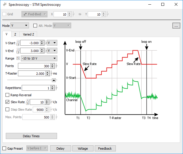
Each datapoint is acquired as an average of several measurements (i.e. oversampled). The sampling rate is 400kHz, so e.g. a 15ms T-Raster would average 6000 measurements per datapoint.
In an ideal world we would use long lock-in time constants and long T-Raster values. However a particularly acute issue for us without a nice stable LT-STM is z-drift of the tip when the feedback loop is disengaged. This is easy to see if Ramp Reversal is selected - if the up and down I(V) traces don’t agree, this is often because the tip has drifted while the feedback loop was turned off. The solution is to measure faster, and compensate by averaging many traces. (This works because the feedback loop is briefly re-engaged between sweeps)
You can go faster by either taking fewer datapoints or using a shorter T-raster time, but as a general rule of thumb don’t make T-raster shorter than 3 lockin time constants. For example, a lockin time constant of 300μs should be paired with a T-raster of at least 1ms. If up/down traces don’t agree in the AUX(V) spectra but they do agree in the I(V) spectra, this is an indication that T-raster is too short.
The other times T1-T4 in an STS sweep are less important - 1ms is a reasonable starting value.
Related to this: in a spatial dI/dV map, the dwell time on each pixel should be at least 3 time constants.
I & V filtering
The Matrix software allows you to turn on low-pass filtering of both VGAP and IT. IT filtering applies only to the feedback loop! This means it has no bearing on STS (the loop is off). VGAP filtering is applied after VEXT modulation has been added. Since low-pass filters have a finite roll-off, you therefore need to stay well clear of the excitation frequency. For example with a 1.3kHz modulation frequency, a 20kHz VGAP filter is OK but 300Hz would completely filter out the lock-in modulation.
Low pass filtering also slows the VGAPsettling time during STS sweeps. In summary, don’t use filtering unless you have a good reason.
Excitation amplitude
The output amplitude displayed on the lockin is VRMS. VP2P is 2.8 times larger.
Some notes recommend using a 20dB or 40dB (10x,100x) attenuation on the lockin output to improve signal-to-noise. The reason for this is the relatively low output resolution on older instruments like the SR830, which has a sineout voltage resolution of 2mV. For small excitations (5-50mV), better resolution is available by using a higher sineout voltage and then dividing it back down with the attenuator. For the newer SR860 lockin this is unnecessary - here the output resolution is 3 digits down to 1nV (so for example, a setting of 50mV has 0.1mV resolution).
For both the SR830 and SR860, sineout has a 50 Ohm output impedance. This means that if you send this signal into a 50 Ohm resistor, you have made a voltage divider and the voltage ‘sags’ - the resistor only sees half the specified voltage. If the signal is sent into a large resistance or high input impedance, the 50 Ohm output impedance becomes negligible and all the voltage is dropped on the thing you’ve plugged it into. The V-EXT input on the matrix box is high impedance, so it is safe to assume that the amplitude the tip is seeing is what the lockin says it is producing.
The SR860 is slighly more complicated since it has a differential output. However it has been designed such that if you only connect to a single output terminal and leave the other open, it behaves like the SR830: feed it to a high input impedance, and the voltage will be what it says on the display.
Typically we operate in the -10..10V VGAP range. When you switch to the -1..1V range, the V:sub:`EXT`input is divided by 10. So if one were configured with 20mV RMS, changing down to the -1..1V range would leave you with only 2mV RMS modulation on the tip.
Acquiring and processing STS
Since we typically need to operate with short measurement times, expect to have to average 50+ traces in order to see anything reasonable. Vernissage is the best way to do the averaging, and can then export the averaged measurement for analysis elsewhere. Due to the way Matrix saves data, scan loading becomes slower the more measurements an experiment contains. It it helpful to start a new experiment (disconnect then reconnect) rather than accumulate hundreds of files.
As a useful sanity check, the lockin signal (AUX1(V)) should be the same as a numerically integrated averaged I(V) trace, just with much less noise. If it’s not, something might be wrong with your lockin settings.
The transmission factor in the usual tunnel current expression introduces a background to STS curves which scales exponentially with the bias voltage and tip-sample separation. A common method to remove this involves normalizing dI/dV to the total conductance I/V, leaving the dimensionless quantity (dI/dV)/(I/V). Sometimes this is written as d(lnI)/d(lnV), which should not be interpreted as dIdV on a log scale. Rather, this is just the lockin AUX1 trace divided by the absolute value of the I-V trace. Here is an example for measurements on Si(111)2x1 by Feenstra et al (https://doi.org/10.1016/0039-6028(87)90170-1):
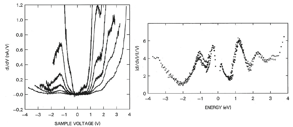
Before doing this division it is essential to manually zero any current offset in the conductance trace, i.e. make I=0 at V=0.
Energy resolution
Instrumental energy resolution in STS is determined by the range of states which contribute to the tunneling current. In the limit of large (>2V) biases, the primary source of resolution broadening is the transmission factor, which scales exponentially with bias voltage. Regardless of any thermal broadening considerations, you cannot do better than several hundred meV resolution in this regime.
In the small voltage regime, the instrumental energy resolution is set by the modulation amplitude of the lock-in detection, and the thermal broadening of the tip Fermi edge. Assuming a constant tip DOS, the thermal broadening comes out to 3.2kT FWHM, which is 80meV at 300K, 30meV at 77K and 15meV at 50K. The modulation voltage broadening is typically taken as 2-2.5 times VRMS.
Since the two contributions add as a sum of squares, reasonable lower bounds estimates for the modulation voltage are:
Tip Temperature (K) |
VRMS (mV) |
Total resolution (meV) |
|---|---|---|
300 |
30 |
110 |
110 |
10 |
40 |
50 |
5 |
20 |
The VT-XA does not cool the tip. It is possible that keeping the tip in tunnel contact to a cooled sample may result in localized cooling, but this is difficult to quantify. Hence for this instrument there would seem to be no point in ever using a modulation voltage lower than 30meV.
An energy resolution of 110meV may not sound appealing, but bear in mind that with the exception of superconductivity features, density of states peaks are usually not especially sharp.
Examples
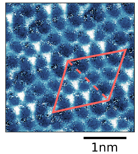
Si(111) 7x7, T=300K
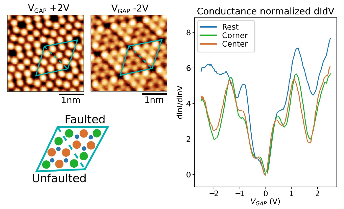
And a corresponding dIdV map (spatial+energy resolved) at a gap voltage of -1eV: